Prototypes to high-volume production
Our partner HiTek’s efficient and flexible machinery supports prototypes and small batches as well as high-volume production. Quality and speed are our priorities so that your projects can move forward quickly.
Services / 01
Customised. Precise. Down to the last detail.
From prototypes to high-volume production: quality PCBs from our exclusive partner HiTek Circuits.
Discuss your project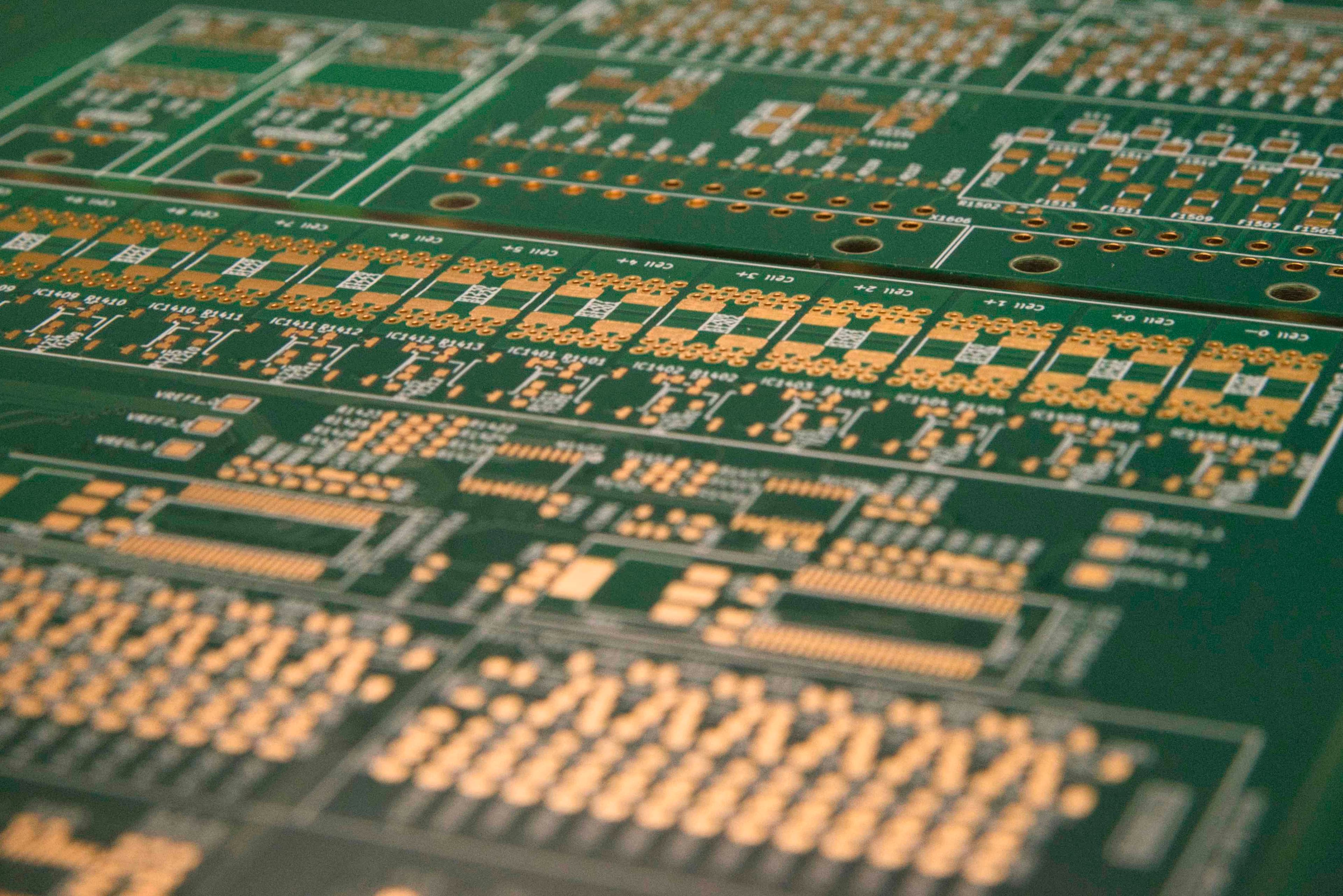
As HiTek Circuits’ exclusive partner, we operate throughout Germany and are your point of contact for all PCB requirements.
BY YOUR SIDE FROM THE START
Our partner HiTek’s efficient and flexible machinery supports prototypes and small batches as well as high-volume production. Quality and speed are our priorities so that your projects can move forward quickly.
Prototypes and small batches can be produced within 5–7 days. High-volume production takes 10–12 days. When every hour counts, express production is available within 24–72 hours.
Our partner HiTek is certified to UL E332365, IATF 16949, ISO 9001 and ISO 14001.
Our experienced team helps you find the right solution for your product. We thoroughly review your documentation and provide feedback on any issues or opportunities for improvement.
Direct communication with HiTek gives you first-hand production feedback. Together, we optimise your documentation and data to suit your finished product.
We remain your direct point of contact after your order is complete. Whatever your last production run, we support you with all questions about your PCBs.
PCB / CAPABILITIES
An overview of the technical capabilities of our manufacturing partner HiTek Circuits.
| Layers | 1–20 layers |
|---|---|
| Base materials | FR4 (high-TG, halogen-free), CEM-1, CEM-3, aluminium, flex, rigid-flex |
| Max. copper weight | 6 oz |
| Min. core thickness | 0.1 mm |
| Surface finishes | LF-HAL, HAL, ENIG, OSP, immersion silver/tin, hard gold, gold fingers |
| Board thickness | 0.3 mm (2 layers) / 0.4 mm (≥4 layers) – 4.0 mm |
| Max. panel size | 635 × 1,500 mm (single-layer); 635 × 1,300 mm (multilayer) |
| Drilling tolerances | Position ±0.075 mm; diameter ±0.05 mm |
| Etching / milling tolerances | ±10% / ±0.1 mm |
| Additional capabilities | BGA, blind vias, laser drilling, Jump V-CUT, carbon ink, HDI, stepped drilling, controlled-depth drilling, back drilling, plugged vias |
LET’S CONNECT
From your first idea through to sourcing. Let’s talk about your next project.